I show the design of the KD202K diffusion silicon diode (9 photos)
Hello, dear readers of my blog. Today we are reviewing (and disassembling =) ) the KD202K diffusion silicon diode. This diode was designed to convert alternating voltage (with a frequency of up to 5 kHz) into direct voltage, that is, in electrical circuits it acted as a rectifier. 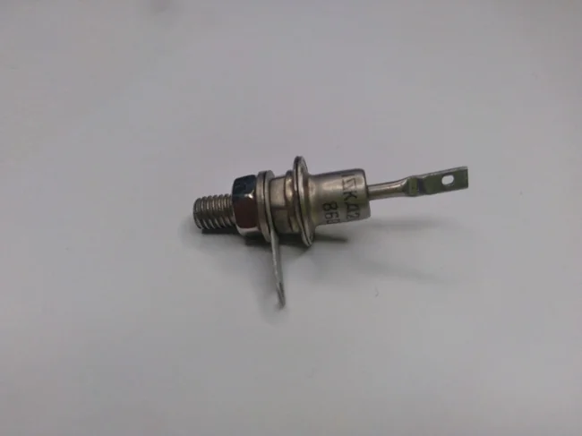
A handsome diode KD202K
The marking of this diode is deciphered as follows:
K - silicon. The first letter in the diode marking characterizes the source material that was used for its development. For example, other options are possible: G - germanium, A - gallium arsenide, I - indium phosphide;
D - diode;
202 - designates the purpose and quality properties of the diode, the serial number of the development. In this case, 202 is a medium-power diode with an average current value from 0.3 to 10 A;
K - classification of this diode within the technological type according to one or more electrical parameters. 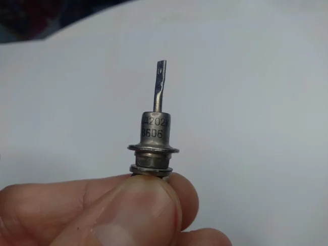
I'm trying to show you the marking of this diode
If we use reference information, then using this marking, we can decipher that KD202K denotes a silicon diffusion rectifier diode with an allowable average forward current of up to 10A. 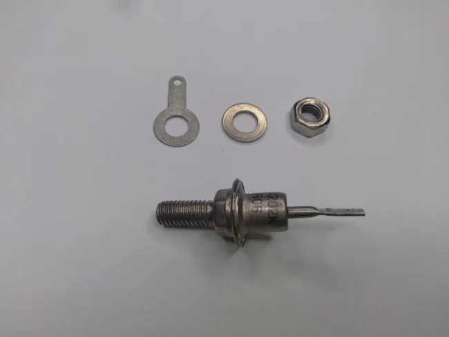
Freed the diode from the "shackles"
Structurally, this diode is made in a metal-glass case and has two external terminals. The lower terminal (cathode) is made in the form of a screw, which also acts as a fastening element of this diode. For the especially curious, the thread is M5. The upper terminal (anode) is made in the form of a rigid terminal, about 1 cm long. 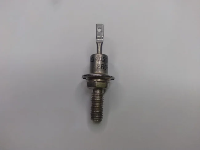
KD202K in all its glory
The metal-glass case in which this diode is placed is typical, has the designation KDYu-11 and a number of diodes are made on its basis. Inside this case is located directly the p-n junction, made in the form of a crystal. p-n junction (electron-hole junction) is the area in which two semiconductors with different types of conductivity (p-type and n-type) come into contact.
p-n junction is created by adding (so-called doping) acceptor impurities on one side of the semiconductor crystal, while the other side is doped with donor impurities. The boundary between these two areas is called a PN junction.
In our case with KD202, as you understand, the crystal is made of silicon. In diffusion diodes, the p-n junction is created at high temperature by the diffusion of impurity into silicon from a medium containing impurity vapors.
The leads are soldered to the areas with p-type and n-type conductivity. The anode is soldered to the p-type zone, and the cathode to the n-type zone. 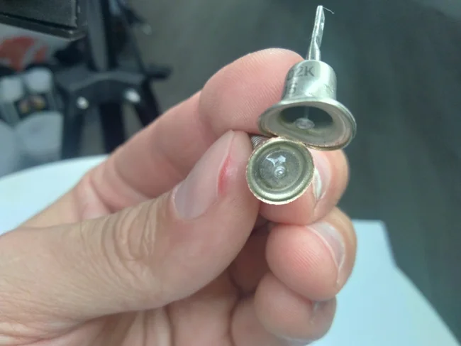
We opened our diole 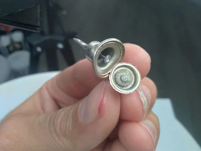
A little from a different angle
Having opened the diode, we can see the crystal placed on the crystal holder. The upper terminal of the diode was soldered to it. It came off during the process of dismantling the upper cover of the housing of this diode. 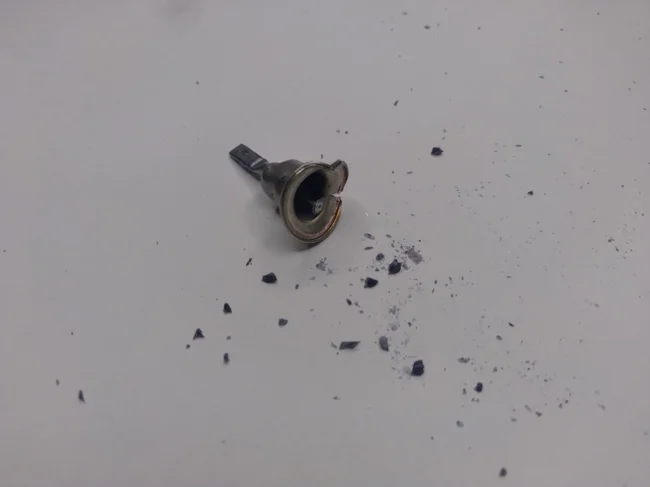
Broken glass insulator
There was a glass insulator in the upper part of the case cover, you can see its fragments in this photo. I squeezed the upper part of the case cover with side cutters and this insulator crumbled into small fragments. 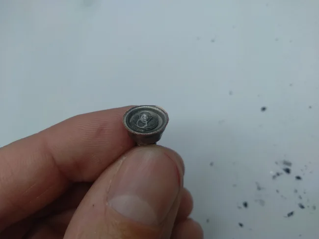
The crystal of this diode itself
At the bottom of the case there is a crystal holder on which the crystal itself is placed. All this magnificence is filled with either a layer of glass or a layer of epoxy resin. It felt more like soft glass. 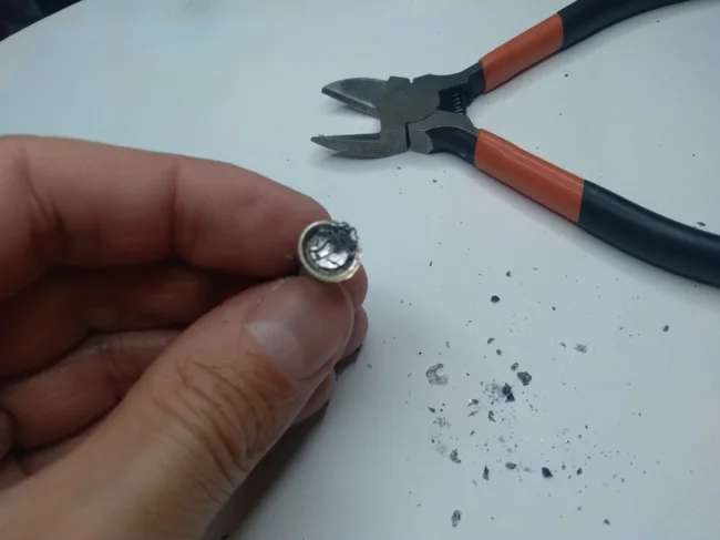
I picked apart the base of the diode under the crystal
If you pick apart the part where the crystal is located, you will find a rather soft metal underneath, which in its consistency resembles lead-tin solder.


